1. Assume that a silicon transistor with β =50, VBEactive=0.7 V, VCC =15V and RC=10K is used in the Fig.1.It is desired to establish a Q-point at VCE=7.5 V and IC=5mA and stability factor S≤5.Find Re,R1and R2.
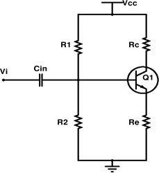
Fig.1
1. Assume that a silicon transistor with β =50, VBEactive=0.7 V, VCC =15V and RC=10K is used in the Fig.1.It is desired to establish a Q-point at VCE=7.5 V and IC=5mA and stability factor S≤5.Find Re,R1and R2.
Fig.1
2. In the Darlington stage shown in Fig.2 , VCC=15V , β1=50, β2=75,VBE=0.7,RC=750 Ω and RE=100 Ω. If at the quiescent point VCE2=6V determine the value of R.
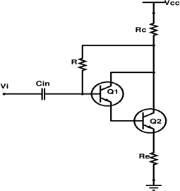
Fig.2
3. For the amplifier shown in Fig.3 using a transistor whose parameters are hie=1100,hre=2.5×10⁻⁴,hfe=50,hoe=24µA/V.Find AI, AV, AVS and Ri.
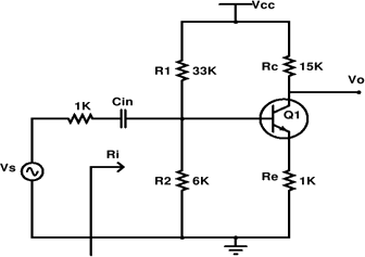
Fig.3
4. Find the voltage gain AV , AVSof the amplifier shown. Assume hie =1100 ,hre=2.5×10⁻⁴, hfe=50, hoe=24µA/V. Also find Ri and Ro.
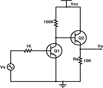
Fig.4
5. Given the following transistor measurements made at IC=10mA , VCE=7.5V and at room temperature hfe=100 , hie =1100 , Aie=40 at 1MHz and Cc=3 pf. Find fβ , fT , Ce , rbꞌe and rbbꞌ.
6. Determine the voltage gain for the following circuits given in Fig.6.
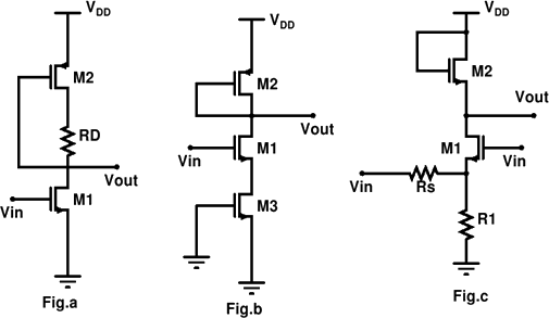
Fig.6
7. Design the circuit given in Fig.7 for a voltage gain of 30 and a power budget of 15mW. Assume voltage drop across Rs is equal to the overdrive voltage of the transistor and RD=400 Ω.
Fig.7
8. In the following amplifier circuit shown in Fig.8 small signal output resistance Rout=Routa//Routb, where Routais the resistance seen from the drain of M2 and Routb is the resistance seen from drain of M3.
If ID1=2ID2
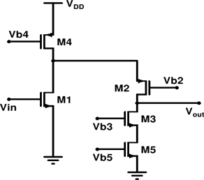
Fig.8
9. The current mirror shown in the Fig.9 should satisfy the following conditions.
for all transistors . Iref =1µA,Iout=10µA.Gate overdrive VGST=200mV for M1and M2.
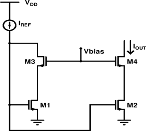
Fig.9
10. Design the commongate stage of the given circuit in Fig.10 which employs the current source M3 as the load to achieve a voltage gain .Neglect λ of M1 . Assuming M3= 400/1 , λn=0.1V-1 , λp = 0.2 V-1,design the circuit for a voltage gain of 100 an input impedance of 200 Ω and a power budget of 30mW.
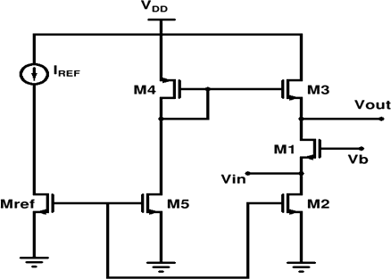
Fig.10
11. Due to manufacturing error,a parasitic resistance RP has appeared in series with the source of M1 as shown in figure . Assume λ =0.Detremine the input and output poles of the circuit and plot the bode diagram.
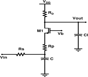
Fig.11
12. Construct the bodeplot of ![]() and find the poles and zeroes.
and find the poles and zeroes.
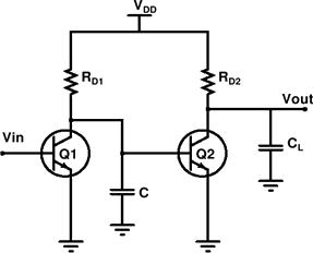
Fig.12
13. Design a PMOS differential amplifier for the following specifications. ![]() =100 , IREF=I=500µA . The dc voltage at the gates of M6 and M7 is 2.5V. The DC voltage at the gate of M7 , M4 and M5 is -2.5 V . The µnCox= 3µpCox=120µA/ V2, Vtn=|Vtp|= 0.7V ,
=100 , IREF=I=500µA . The dc voltage at the gates of M6 and M7 is 2.5V. The DC voltage at the gate of M7 , M4 and M5 is -2.5 V . The µnCox= 3µpCox=120µA/ V2, Vtn=|Vtp|= 0.7V ,![]() = |
= |![]() |=30V.
|=30V.
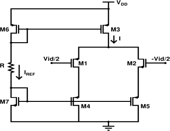
Fig.13
14. For the given circuit in Fig.14 draw the half circuit for both differential and common mode and compute both differential and common mode gain.
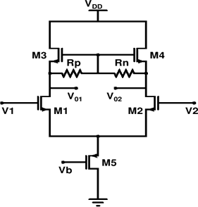
Fig.14
15. For the given circuit in Fig.15 draw the half circuit for both differential and commonmode and compute both differential and common mode gain.
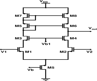
Fig.15
16. A typical differential Amplifier shown in Fig.16 has interesting combination of loads which is parallel combination of current source load and diode connected load. Evaluate Vout =V01 - V02 and differential gain Avdm.Given λn =0.04/V,λp=0.06/V , M1= M2=50/0.5 ,Iss=5mA, βnꞌ=50uA/V2 βpꞌ=16µA/V2,M3=M4=10/0.5,M5=M6=40/0.5.What would have been Avdm value if the loads are only diode connected load instead of M3 & M5 combination.
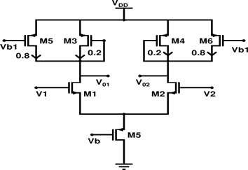
Fig.16
17. Design all of the W/L values of every transistor of this opamp to meet the following specifications :
Find differential gain, power dissipation and VBp & VBn.
SR= ±20V/µs , ![]() =3V ,
=3V , ![]() =0.8V,
=0.8V, ![]() =1.2V ,
=1.2V , ![]() =3V and
GB=40MHz.
=3V and
GB=40MHz.
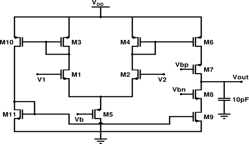
Fig.17
18. . In the two stage feedback amplifier shown in Fig.18 , the transistors are identical and have hfe=100 and hre=10K Ω, hre=0and hoe =0.Calculate
i)Aif=Io/Is
ii)Rif=Vi/Is
iii)Aꞌif=Io/Iiꞌ,
iv)Avf=Vo/Vs where Vs=IsRs
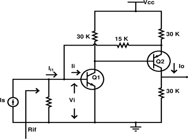
Fig.18
19. For the given circuit shown in Fig.19 ,assume λ =0
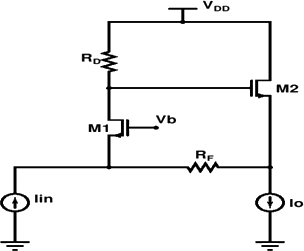
Fig.19
20. Consider the feedback circuit shown in Fig.20, assume VA=α
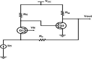
Fig.20
21. For the given circuits
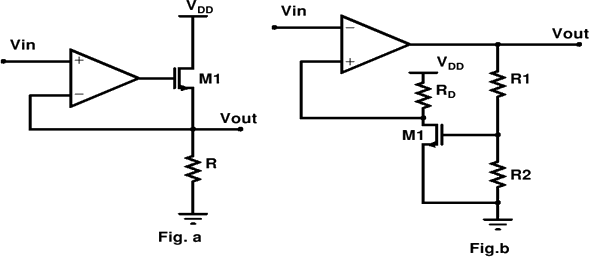
Fig.21
22. . Design an opamp circuit to provide an outputVo = -(6V1+ ![]() +
+ ![]() . Choose relatively low values of resistances but ones for which the input current (from each input signal source) does not exceed 0.1mAfor 1V input signal.
. Choose relatively low values of resistances but ones for which the input current (from each input signal source) does not exceed 0.1mAfor 1V input signal.
23. For the given circuit in Fig.23 find ![]() .
.
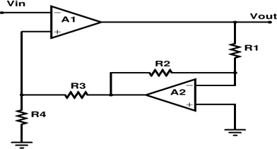
Fig.23
24. For the given opamp circuit in Fig.24
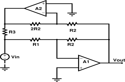
Fig.24
25. Design a bandpass filter with fo=1MHz and Q=10 and unity resonance gain. Find HOBP,ωO and Q for C1=C2=Cand R1=R2=R.
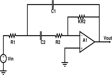
Fig.25
26. The circuit shown in Fig.26 uses a summing amplifier A1 and a bandpass stage A2 to increase the Q of the bandpass stage without changing ωo.This allows for high QS without unduly taxing A2.
 and
and 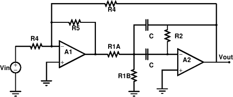
Fig.26
27. We wish to design a quartz crystal oscillator of frequency 2 MHz. Draw equivalent resonant tuned circuit for such crystal. If ![]() and series resonant
and series resonant ![]() . Evaluate
. Evaluate ![]() and Q. The crystal is to be used in colpitt oscillator. In that configuration the MOS transistor is biased to
and Q. The crystal is to be used in colpitt oscillator. In that configuration the MOS transistor is biased to ![]() 2 mA. We have
2 mA. We have ![]() =100
=100![]() .Evaluate value of resistance R shunting across drain and source of transistor and value of
.Evaluate value of resistance R shunting across drain and source of transistor and value of ![]() . The colpitts oscillator with quartz crystal has the circuit as shown in Fig.27. Assume
. The colpitts oscillator with quartz crystal has the circuit as shown in Fig.27. Assume ![]() = 0.02 pf.
= 0.02 pf.
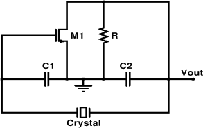
Fig.27
